(China (Mainland))


Product Summary
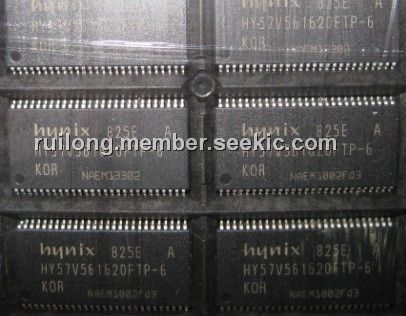
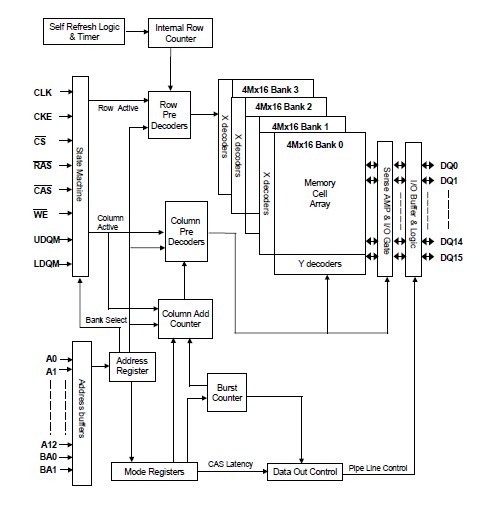
The HY57V561620FTP-6 is a 268,435,456 bit CMOS Synchronous DRAM, ideally suited for the main memory applications which require large memory density and high bandwidth. It is organized as 4banks of 4,194,304x16. The HY57V561620FTP-6 is offering fully synchronous operation referenced to a positive edge of the clock. All inputs and outputs are synchronized with the rising edge of the clock input. The data paths are internally pipelined to achieve very high bandwidth. All input and output voltage levels are compatible with LVTTL.
Parametrics
HY57V561620FTP-6 absolute maxing ratings: (1)Ambient Temperature TA: -40~85℃; (2)Storage Temperature TSTG: -55 ~ 125℃; (3)Voltage on Any Pin relative to VSS VIN, VOUT: -1.0 ~ 4.6V; (4)Voltage on VDD relative to VSS VDD, VDDQ: -1.0 ~ 4.6V; (5)Short Circuit Output Current IOS: 50mA; (6)Power Dissipation PD: 1W; (7)Soldering Temperature Time TSOLDER: 260.10℃ Sec.
Features
HY57V561620FTP-6 features: (1)Single 3.3±0.3V power supply; (2)All device pins are compatible with LVTTL interface; (3)JEDEC standard 400mil 54pin TSOP-II with 0.8mm of pin pitch; (4)All inputs and outputs referenced to positive edge of system clock; (5)Data mask function by UDQM, LDQM; (6)Internal four banks operation; (7)Auto refresh and self refresh; (8)8192 refresh cycles / 64ms; (9)Programmable Burst Length and Burst Type: - 1, 2, 4, 8 or Full page for Sequential Burst; - 1, 2, 4 or 8 for Interleave Burst; (10)Programmable CAS Latency ; 2, 3 Clocks; (11)?Ambient Temperature : - 40 ~ 85℃.
Diagrams
T") |
 HY57V121620(L)T |
Other |
|
Data Sheet |
Negotiable |
|
||||
|
HY57V161610D |
Other |
|
Data Sheet |
Negotiable |
|
||||
|
HY57V161610D-I |
Other |
|
Data Sheet |
Negotiable |
|
||||
|
HY57V161610E |
Other |
|
Data Sheet |
Negotiable |
|
||||
|
HY57V161610ET-I |
Other |
|
Data Sheet |
Negotiable |
|
||||
|
HY57V161610ETP-I |
Other |
|
Data Sheet |
Negotiable |
|
||||